New atom-thin material solves major semiconductor wiring problem
📊Executive Summary
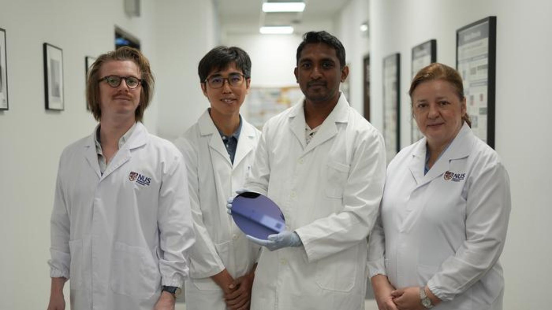
Researchers at the National University of Singapore and Applied Materials have developed a groundbreaking method for growing extremely thin tungsten disulfide films, only 0.7 nanometers thick, to protect copper wiring in microchips. This innovation addresses the issue of bulky insulation materials that hinder chip performance by increasing electrical resistance. The new film acts as both a barrier and liner, significantly reducing the coating's footprint and extending the lifespan of the wiring under extreme electrical stress. As global chip demand approaches $1 trillion annually, this advancement is timely and meets stringent manufacturing standards, potentially impacting semiconductor production and procurement strategies....
More Insights Available
Unlock Full Analysis
Sign in to access the complete executive brief, risk analysis, and full article content.